Why Upgrade to 6 Layers?
When a 4-layer PCB no longer suffices, it’s time to consider a 6-layer board. The additional layers offer several benefits:
- More signal routing space
- An extra plane pair
- Flexibility in conductor arrangement
The key to success lies in the PCB stackup arrangement and routing strategy.
6-Layer PCB Stackup Selector 6L
Configure layer thicknesses for your 6-layer PCB stackup
Copper Layers
Prepreg Layers
Core Layers
Total Board Thickness
1.200mm
1200 µm
vs 1.2mm target:
+0 µm
| Component | Thickness |
|---|---|
| Copper (6 layers) | 210 µm |
| Prepreg (3 layers) | 456 µm |
| Core (2 layers) | 400 µm |
Stackup Visualization
SOLDER MASK (TOP)
L1 – Top SignalOUTER
35µm
Prepreg 1 (PP1)
114µm
L2 – GND PlanePLANE
35µm
Core 1 (FR-4)
200µm
L3 – Inner SignalSIGNAL
35µm
Prepreg 2 (PP2)
228µm
L4 – Inner SignalSIGNAL
35µm
Core 2 (FR-4)
200µm
L5 – PWR PlanePLANE
35µm
Prepreg 3 (PP3)
114µm
L6 – Bottom SignalOUTER
35µm
SOLDER MASK (BOTTOM)
Outer Copper
Plane (GND/PWR)
Inner Signal
Prepreg (PP)
Core (FR-4)
Solder Mask
💡 Common 6-Layer Targets
1.0mm: High-density, compact designs
1.2mm: Standard thin multilayer
1.6mm: Most common thickness
2.0mm: Power applications, thermal management
1.2mm: Standard thin multilayer
1.6mm: Most common thickness
2.0mm: Power applications, thermal management
⚡ Layer Arrangement Tips
L2 (GND) & L5 (PWR): Place planes adjacent to outer signal layers for better impedance control and EMI shielding.
L3 & L4: Inner signal layers – route high-speed signals here for protection.
L3 & L4: Inner signal layers – route high-speed signals here for protection.
Reasons to Choose a 6-Layer Board
- More surface space: Moving power and signal layers inside frees up room for components on the surface.
- Mixed-signal boards: Dedicate a surface layer to analog interfaces and use an internal layer for slower digital routing.
- High-speed, high I/O count boards: Separate signals into different layers for better organization.
Typical 6-Layer PCB Stackup
A common 6-layer stackup arrangement:
- Signal (Top)
- Ground
- Power
- Signal
- Ground
- Signal (Bottom)
Signal Routing Guidelines
- Use top and bottom layers for impedance-controlled signals.
- Thin dielectrics (≤10 mil) are preferable for these outer layers.
- For digital interfaces with differential pairs, reduced trace width allows routing to fine-pitch components.
Power Routing Strategies
- Dedicate an internal layer to power distribution.
- Break up the power plane into rails for multiple voltages if needed.
- You can still route power on signal layers using copper pour or thick traces when necessary.
High Current Considerations
For high current applications:
- Use two internal power layers interleaved with ground.
- Consider using the back layer as an additional power plane for increased current handling.
3-Core vs. 2-Core Stackup
A 3-core (or 1 thick central core with thin outer layers) arrangement is often superior:
- Increases PDN plane capacitance
- Reduces spreading inductance
- Minimizes radiated emissions from PCB edge
- Provides more consistent impedance for signals on L4

Best Practices
- Get your stackup approved by a fabrication house before layout and routing.
- Apply EMC strategies used in 4-layer and 8-layer boards.
- Consider DFM (Design for Manufacturing) guidelines throughout the process.
Remember, the stackup arrangement significantly impacts EMC and signal integrity, so choose wisely based on your specific application needs.
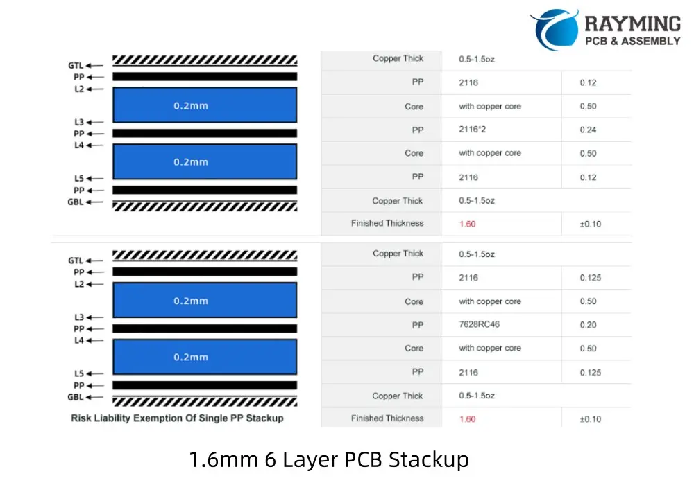
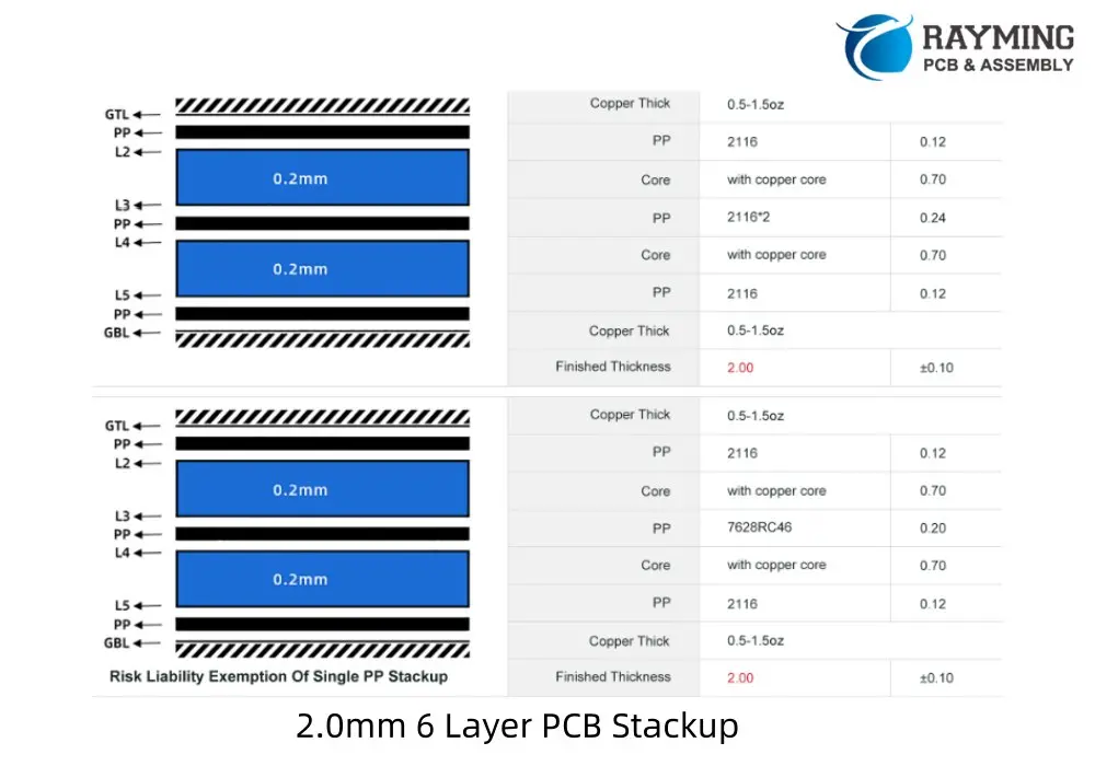
6 Layer PCB stackup reference for different thickness:
- Read more about: 4 Layer PCB Stackup


If you need stackup suggestion for your 6 layer PCB design, welcome to contact us.