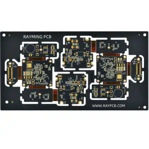
Introduction
In today’s digital age, Printed Circuit Boards (PCBs) are the backbone of nearly every electronic device we use. From smartphones to satellites, PCBs play a crucial role in connecting and supporting electronic components. Understanding the PCB manufacturing process is essential for engineers, designers, and anyone involved in the electronics industry. This comprehensive guide will walk you through the intricate steps of PCB manufacturing, providing insights into the technology, challenges, and best practices in this field.
What is PCB Manufacturing?

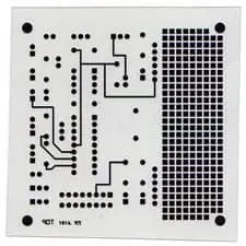
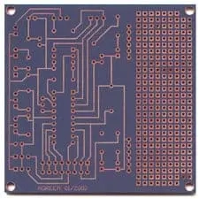
PCB manufacturing is the process of creating printed circuit boards that mechanically support and electrically connect electronic components using conductive pathways, tracks, or signal traces etched from copper sheets laminated onto a non-conductive substrate. This process involves multiple steps, combining precision engineering, chemistry, and advanced technology to produce boards that meet the exacting standards of modern electronics.
Learn More about:
- PCB Assembly Process
- Flex PCB Manufacturing Process
- Rigid Flex PCB Manufacturing Process
- Ceramic PCB Manufacturing Process
- Aluminum PCB Manufacturing Process
Key Aspects of PCB Manufacturing:
- Substrate Material Selection: Choosing the right base material, typically FR-4 (a glass-reinforced epoxy laminate).
- Copper Layering: Applying thin copper foils to the substrate.
- Circuit Design Transfer: Transferring the designed circuit pattern onto the copper layers.
- Etching: Removing unwanted copper to create the circuit paths.
- Layering: For multi-layer boards, bonding multiple layers together.
- Drilling: Creating holes for component connections and vias.
- Surface Finishing: Applying protective coatings and final touches.
Now, let’s dive into the detailed steps of the PCB manufacturing process.
PCB Manufacturing Process Guide
RAYPCB Engineering Tools
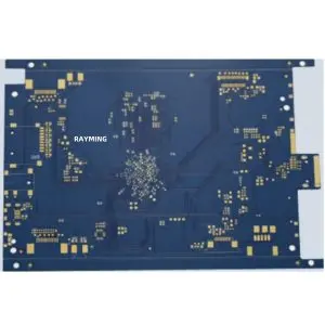
2-Layer PCB Manufacturing Process
The standard PCB manufacturing process for double-sided circuit boards. This process involves creating conductive patterns on both sides of a substrate with through-hole connections.
Design Data Preparation CAM
Import Gerber files, drill files (Excellon), and perform Design Rule Check (DRC). Generate tooling holes and panelization for efficient production.
Material Cutting & Preparation LAMINATE
Cut copper-clad laminate (CCL) to panel size. FR-4 glass epoxy is standard, with copper foil thickness typically 1oz (35μm) or 2oz (70μm).
Inner Layer Imaging PHOTOLITHOGRAPHY
Apply dry film photoresist, expose using LDI (Laser Direct Imaging) or conventional exposure with photomask, then develop to create circuit pattern.
Etching CHEMICAL
Remove unwanted copper using chemical etchant (typically CuCl₂ or FeCl₃ based), leaving only the protected circuit traces. Strip remaining photoresist.
AOI Inspection QUALITY
Automated Optical Inspection to detect opens, shorts, missing features, and other defects before proceeding to drilling.
CNC Drilling MECHANICAL
High-speed drilling for through-holes and component holes using carbide drill bits. Multiple hit counts tracked for tool life management.
Electroless Copper Deposition PLATING
Desmear, activate, and deposit thin electroless copper layer (0.5-1μm) on hole walls to establish conductivity for subsequent electroplating.
Electrolytic Copper Plating PLATING
Build up copper thickness in holes (PTH) and on surface. Target plating thickness typically 20-25μm in holes per IPC-6012 Class 2.
Solder Mask Application COATING
Apply liquid photoimageable solder mask (LPI/LPISM), expose, develop to protect copper and define solderable areas.
Surface Finish FINISHING
Apply protective finish to exposed copper pads. Options include HASL, ENIG, OSP, Immersion Silver, or Immersion Tin based on application.
Silkscreen Legend MARKING
Print component reference designators, logos, and other markings using inkjet or screen printing with epoxy-based ink.
Electrical Test & Profiling FINAL QC
Flying probe or fixture test for opens/shorts. CNC routing to final board dimensions with V-scoring or tab routing for arrays.
Standard Specifications
- Board Thickness 0.4-3.2mm
- Copper Weight 0.5-6 oz
- Min Trace/Space 3/3 mil
- Min Drill Size 0.15mm
- Aspect Ratio 10:1
- Surface Finish Multiple
Quality Standards
- IPC-A-600 Acceptability
- IPC-6012 Qualification
- IPC-2221 Design
- UL 94V-0 Flammability
- RoHS Compliant
- ISO 9001 Certified
Common Applications
- Consumer Electronics High Vol
- LED Lighting Standard
- Power Supplies Heavy Cu
- IoT Devices Compact
- Automotive Reliable
- Industrial Control Robust
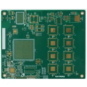
Multilayer PCB Manufacturing Process
Advanced PCB manufacturing for 4+ layer boards requiring lamination of multiple inner layers with prepreg and copper foil. Essential for high-density designs and impedance control.
Design Review & Stackup Definition ENGINEERING
Define layer stackup, material selection, and impedance requirements. Calculate prepreg/core thicknesses for target impedance values.
Inner Layer Core Preparation MATERIAL
Cut thin core laminate (typically 0.1-0.5mm) with copper on both sides. Clean and prepare for imaging process.
Inner Layer Imaging PHOTOLITHOGRAPHY
Apply photoresist, expose inner layer patterns using high-precision LDI, and develop. Critical for layer-to-layer registration.
Inner Layer Etching CHEMICAL
Etch away exposed copper to form inner layer circuitry. Etch factor control critical for fine-pitch designs.
AOI Inner Layer Inspection QUALITY
100% automated optical inspection of inner layers before lamination. Defects cannot be repaired after lamination.
Oxide/Brown Oxide Treatment SURFACE PREP
Create micro-rough copper surface for enhanced bonding with prepreg during lamination. Black oxide or alternative treatments.
Layup & Registration LAMINATION
Stack inner layers with prepreg sheets and outer copper foil in precise alignment using pins or mass lamination systems.
Vacuum Lamination Press LAMINATION
Apply heat and pressure in vacuum press to cure prepreg and bond all layers into solid multilayer structure.
X-Ray Drilling & Target Drill ALIGNMENT
Use X-ray to locate inner layer registration targets. Drill precision tooling holes for outer layer alignment.
Mechanical & Laser Drilling DRILLING
Drill through-holes mechanically. Use CO₂/UV laser for blind/buried vias and microvias in HDI designs.
Desmear & Electroless Copper PLATING
Remove drilling smear from hole walls and deposit seed copper layer for subsequent electroplating.
Pattern Plating & Etching PLATING
Image outer layers, electroplate copper and tin, then etch to create final outer layer circuit pattern.
Solder Mask, Finish & Test FINAL
Apply solder mask, surface finish, silkscreen. Electrical test with TDR impedance verification for controlled impedance boards.
Multilayer Capabilities
- Layer Count 4-40+ layers
- Min Trace/Space 2/2 mil
- Laser Via Size 75μm
- Aspect Ratio 15:1
- Registration ±2 mil
- Impedance Tolerance ±10%
Advanced Materials
- High-Speed Megtron 6/7
- RF/Microwave Rogers RO4350B
- High-Tg TG170+ FR-4
- Halogen-Free Available
- Low-Dk Dk 3.0-3.5
- Metal Core Aluminum/Copper
HDI Structures
- 1+N+1 Standard HDI
- 2+N+2 Advanced HDI
- Any-Layer ELIC
- Via-in-Pad Filled & Capped
- Stacked Vias Up to 4
- Skip Vias Supported
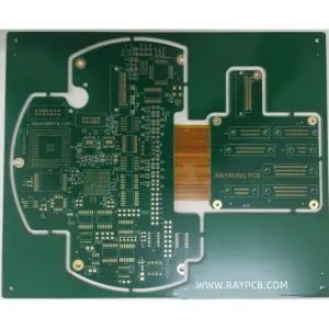
Flex PCB Manufacturing Process
Flexible circuit manufacturing using polyimide substrates. Requires specialized handling and processes to maintain dimensional stability and flexibility.
Design Analysis & Material Selection ENGINEERING
Evaluate bend radius, flex cycles, and dynamic vs static flex requirements. Select appropriate polyimide and adhesive system.
Polyimide Film Preparation MATERIAL
Cut copper-clad polyimide laminate. Pre-bake to remove moisture and stabilize dimensional properties.
Drilling & Plasma Desmear DRILLING
UV laser or mechanical drilling for vias. Plasma treatment removes polyimide smear and improves plating adhesion.
Metallization & Plating PLATING
Electroless copper seeding followed by electrolytic copper build-up. Lower temperatures than rigid PCB processes.
Imaging & Etching PATTERNING
Apply photoresist with scale compensation, expose circuit pattern, and etch with precise control for fine features.
AOI & Coverlay Application COATING
Inspect circuits, then apply polyimide coverlay using vacuum lamination. Critical for flex reliability.
Stiffener & Surface Finish FINISHING
Attach stiffeners for component support, apply ENIG surface finish (no HASL due to thermal stress).
Electrical Test & Singulation FINAL QC
Flying probe test with soft probes, laser or die cutting for final profiling, flex cycle testing for critical applications.
Flex Specifications
- Polyimide Thickness 12.5-125μm
- Copper Type ED or RA
- Min Bend Radius 1mm
- Flex Cycles 1M+ dynamic
- Min Trace/Space 2/2 mil
- Operating Temp -200 to 400°C
Material Options
- Standard PI Kapton®
- LCP High-frequency
- Adhesive Acrylic/Epoxy
- Adhesiveless Best flex life
- FR (Flame Retardant) UL 94 VTM-0
- Coverlay PI + Adhesive
Applications
- Mobile Devices Smartphones
- Medical Implants Pacemakers
- Aerospace Satellites
- Wearables Smartwatches
- Automotive Sensors
- Industrial Robotics
PCB Manufacturing Process Comparison
Compare key differences between 2-layer, multilayer, and flex PCB manufacturing processes to select the right technology for your application.
| Process Parameter | 2-Layer PCB | Multilayer PCB | Flex PCB |
|---|---|---|---|
| Base Material | FR-4 Glass Epoxy | FR-4, High-Tg, Rogers | Polyimide (Kapton®) |
| Layer Count | 2 layers | 4-40+ layers | 1-12 layers |
| Lamination Process | None (single laminate) | Multiple lamination cycles | Coverlay lamination |
| Via Types | Through-hole only | Through, blind, buried, microvias | Through, blind vias |
| Drilling Method | Mechanical CNC | Mechanical + Laser | UV Laser + Mechanical |
| Min Trace/Space | 3/3 mil (75μm) | 2/2 mil (50μm) | 2/2 mil (50μm) |
| Protective Coating | LPI Solder Mask | LPI Solder Mask | Polyimide Coverlay |
| Typical Lead Time | 5-7 days | 10-15 days | 12-20 days |
| Key Challenges | Limited routing, thermal | Registration, impedance control | Dimensional stability, handling |
| Cost Factor | 1x (baseline) | 2-5x (layer dependent) | 3-8x (complexity dependent) |
| IPC Standard | IPC-6012 | IPC-6012 | IPC-6013 |
| Surface Finish Options | HASL, ENIG, OSP, ImSn, ImAg | HASL, ENIG, OSP, ENEPIG | ENIG, OSP, ImSn (no HASL) |
Understanding the PCB Manufacturing Process
The PCB manufacturing process is a complex series of steps that transforms raw materials into functional printed circuit boards. Whether producing simple 2-layer boards, complex multilayer PCBs with high-density interconnects, or flexible circuits for dynamic applications, each technology requires specialized equipment, materials, and expertise.
Key Stages in PCB Board Manufacturing
All PCB fabrication processes share common fundamental stages: design data preparation, substrate preparation, pattern imaging, copper etching, drilling, plating, and surface finishing. However, the specific techniques and equipment vary significantly based on the board type and complexity.
Quality Standards in PCB Fabrication
Professional PCB manufacturers follow strict quality standards including IPC-A-600 for acceptability, IPC-6012 for rigid board qualification, and IPC-6013 for flexible circuit qualification. These standards ensure consistent quality and reliability across the industry.
Choosing the Right PCB Technology
Selection depends on factors including circuit complexity, space constraints, environmental requirements, signal integrity needs, and cost considerations. 2-layer PCBs suit simple designs, multilayer boards enable complex high-speed circuits, and flex PCBs solve space and dynamic flexing challenges.
Ready to Start Your PCB Project?
Get professional PCB manufacturing with fast turnaround, competitive pricing, and engineering support for your 2-layer, multilayer, or flex circuit requirements.
Learn More About PCB Manufacturing ProcessPCB Manufacturing Process – 22 Steps

Step 1: Design and Output
The PCB manufacturing process begins with the design phase. Engineers use Computer-Aided Design (CAD) software to create the circuit layout. This design is then converted into a format that manufacturing equipment can understand, typically Gerber files.
Key Points:
- Circuit schematic creation
- Component placement and routing
- Design Rule Check (DRC)
- Generation of Gerber files and drill data
Step 2: PPE – Pre Production Engineering
Before actual production begins, the design undergoes a thorough review to ensure manufacturability and to identify any potential issues.
Activities in PPE:
- Design for Manufacturing (DFM) check
- Stack-up design for multi-layer boards
- Panelization planning
- Tool and process selection
Step 3: From File to Film
In this step, the digital design is transferred to a physical film, which serves as a template for creating the circuit pattern on the PCB.
Process Details:
- Photoplotter usage for film creation
- Negative or positive image generation based on design requirements
- Film inspection for accuracy
Step 4: Board Cutting (Copper Clad Laminate Cutting)
Raw PCB material, typically copper-clad laminate, is cut to the required panel size.
Considerations:
- Precision cutting to ensure correct dimensions
- Material handling to prevent damage or contamination
Step 5: Printing the Inner Layers
For multi-layer PCBs, this step involves creating the internal circuit layers.
Techniques Used:
- Photoresist application
- UV light exposure through the film mask
- Development of the photoresist
Step 6: Etch Inner Layers

Unwanted copper is removed from the inner layers through chemical etching.
Etching Process:
- Chemical bath application
- Controlled etching to maintain circuit integrity
- Removal of remaining photoresist
Step 7: Inner Layer Alignment
Ensuring precise alignment of inner layers is crucial for multi-layer PCBs.
Alignment Methods:
- Optical alignment systems
- Registration hole punching
- Layer stack-up preparation
Step 8: Automatic Optical Inspection (AOI) Inspection
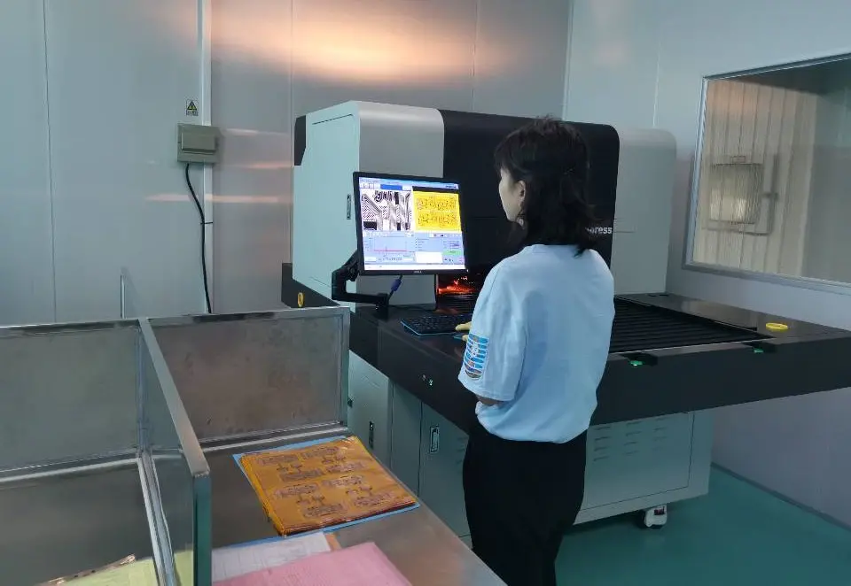
Each inner layer undergoes AOI to detect any defects or inconsistencies.
Inspection Criteria:
- Circuit pattern accuracy
- Copper trace width and spacing
- Absence of shorts or opens
Step 9: Layer-up and Bond
For multi-layer PCBs, the individual layers are stacked and bonded together.
Bonding Process:
- Layer stacking with prepreg sheets
- Application of heat and pressure in a lamination press
- Curing to create a solid multi-layer board
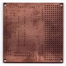
Step 10: Drilling the PCB
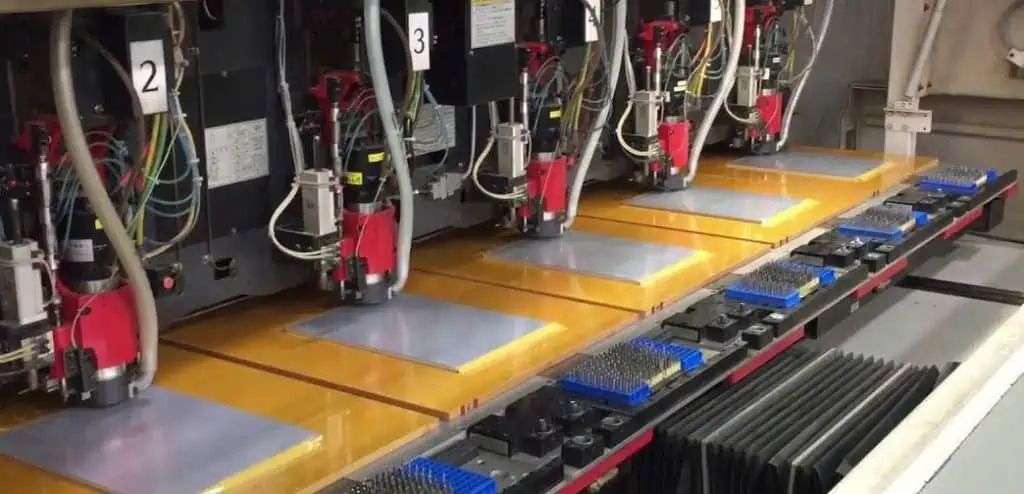
Holes are drilled for component leads, vias, and mounting purposes.
Drilling Techniques:
- CNC drilling for precision
- Laser drilling for micro vias
- X-ray drilling for buried vias in multi-layer boards
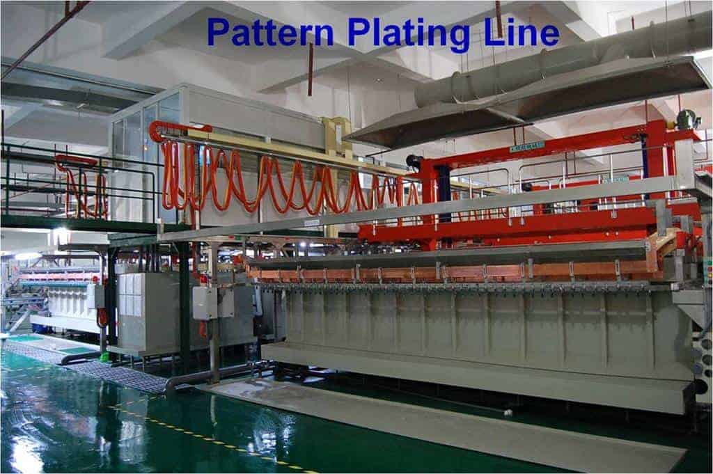
Step 11: Plating and Copper Deposition
This step involves depositing a thin layer of copper over the entire board, including the drilled holes.
Plating Methods:
- Electroless copper deposition
- Electrolytic copper plating
- Through-hole plating for electrical connectivity
Step 12: Outer Layer Imaging
Similar to inner layer imaging, the outer layer circuit pattern is created.
Imaging Process:
- Dry film lamination
- UV exposure using artwork
- Development of the resist pattern
Step 13: Plating
Additional copper is plated onto exposed areas to build up the required copper thickness.
Plating Considerations:
- Copper thickness requirements
- Uniform plating distribution
- Plating of surface mount pads
Step 14: Etch Outer Layer
Unwanted copper is removed from the outer layers, leaving the desired circuit pattern.
Etching Techniques:
- Chemical etching
- Mechanical etching for fine-line requirements
- Differential etching for varied copper thicknesses
Step 15: Outer Layer AOI
Another round of AOI is performed to ensure the accuracy of the outer layer circuits.
Inspection Focus:
- Circuit pattern integrity
- Copper thickness uniformity
- Absence of under-etching or over-etching
Step 16: Solder Mask Application

A protective layer is applied to insulate the copper traces and prevent solder bridges.
Solder Mask Process:
- Solder mask ink application
- UV curing
- Development to expose pads and vias
Step 17: Surface Finish
Various finishes are applied to protect exposed copper and enhance solderability.
Common Finishes:
- Hot Air Solder Leveling (HASL)
- Electroless Nickel Immersion Gold (ENIG)
- Immersion Tin
- Organic Solderability Preservative (OSP)
Step 18: Silkscreen Printing

Component designators, logos, and other markings are printed on the board.
Silkscreen Considerations:
- Ink type selection
- Curing process
- Alignment with board features
Step 19: Electrical Test

Each board undergoes electrical testing to ensure proper connectivity and isolation.
Testing Methods:
- Flying probe testing
- Bed of nails testing
- Continuity and isolation checks
Step 20: Profiling and V-Scoring
Boards are cut to their final shape, and V-scoring is applied for easy separation of panelized boards.
Profiling Techniques:
- CNC routing
- Laser cutting for precision requirements
- V-groove scoring for break-apart panels
Step 21: Final Inspection
A thorough visual and functional inspection is performed before packaging.
Inspection Points:
- Physical dimensions
- Surface finish quality
- Silkscreen accuracy
- Overall board integrity
Step 22: Packaging
Boards are carefully packaged to protect them during shipping and storage.
Packaging Considerations:
- Moisture-sensitive packaging for certain finishes
- ESD protection
- Proper labeling and documentation
2 Layer Vs. Multilayer Manufacturing Process
While the basic principles remain the same, there are significant differences between manufacturing 2-layer and multilayer PCBs.
2-Layer PCB Manufacturing:
- Simpler process with fewer steps
- No inner layer processing required
- Generally faster and more cost-effective
Multilayer PCB Manufacturing:
- More complex with additional steps for inner layers
- Requires precise layer alignment and bonding
- Involves advanced techniques for buried and blind vias
- Offers higher circuit density and better EMI shielding
What is the Difference Between PCB Manufacturing and PCB Assembly Process?
It’s important to distinguish between PCB manufacturing and PCB assembly, as they are two distinct processes in creating a functional electronic device.
PCB Manufacturing:
- Focuses on creating the bare PCB
- Involves all steps from design to final board production
- Ends with a bare board ready for component mounting
PCB Assembly:
- Begins with a completed bare PCB
- Involves placing and soldering components onto the board
- Includes processes like solder paste application, component placement, reflow soldering, and testing of the assembled board
8 Best DFM Tips for PCB Manufacturing

Design for Manufacturing (DFM) is crucial for ensuring smooth production and high-quality PCBs. Here are eight essential DFM tips:
- Optimize Trace Widths and Spacing: Adhere to manufacturer capabilities for minimum trace width and spacing.
- Consider Copper Pour: Use copper pours for ground planes and improved thermal management.
- Plan Via Placement Carefully: Avoid vias in pads when possible and use appropriate via sizes.
- Mind the Edge Clearance: Leave sufficient space between components and board edges.
- Use Standard Drill Sizes: Stick to standard drill sizes to reduce manufacturing costs.
- Consider Panelization: Design with panelization in mind for efficient production.
- Implement Proper Silkscreen Design: Ensure silkscreen text is readable and doesn’t overlap with solder mask openings.
- Follow Stack-up Guidelines: Work with your manufacturer to design an appropriate layer stack-up for multilayer boards.
Trends and Challenges in PCB Manufacturing Technology
The PCB manufacturing industry is constantly evolving, driven by advancements in technology and changing market demands.
Current Trends:
- Miniaturization: Increasing demand for smaller, denser PCBs.
- Flexible and Rigid-Flex PCBs: Growing popularity in wearable and IoT devices.
- High-Frequency Materials: Adoption of advanced materials for 5G and high-speed applications.
- Additive Manufacturing: Exploration of 3D printing technologies for PCB production.
- Green Manufacturing: Focus on environmentally friendly processes and materials.
Challenges:
- Increasing Complexity: Managing the complexity of high-density interconnect (HDI) boards.
- Material Limitations: Overcoming the limitations of traditional PCB materials.
- Cost Pressures: Balancing cost-effectiveness with advanced manufacturing requirements.
- Quality Control: Maintaining high quality standards with increasing miniaturization.
- Skilled Labor Shortage: Addressing the need for skilled technicians in advanced PCB manufacturing.
Conclusion
The PCB manufacturing process is a complex, multi-step journey that transforms a simple design into a sophisticated electronic component. From the initial design phase to the final packaging, each step requires precision, expertise, and attention to detail. As technology continues to advance, PCB manufacturers must adapt to new challenges while maintaining the high standards of quality and reliability that modern electronics demand.
Understanding this process is crucial for anyone involved in electronics design or production. By following best practices in Design for Manufacturing and staying abreast of industry trends, engineers and manufacturers can ensure the production of high-quality, cost-effective PCBs that meet the ever-evolving needs of the electronics industry.
As we look to the future, the PCB manufacturing process will undoubtedly continue to evolve, driven by the relentless pursuit of smaller, faster, and more efficient electronic devices. The industry’s ability to innovate and overcome challenges will play a crucial role in shaping the next generation of electronic products that will power our increasingly connected world.