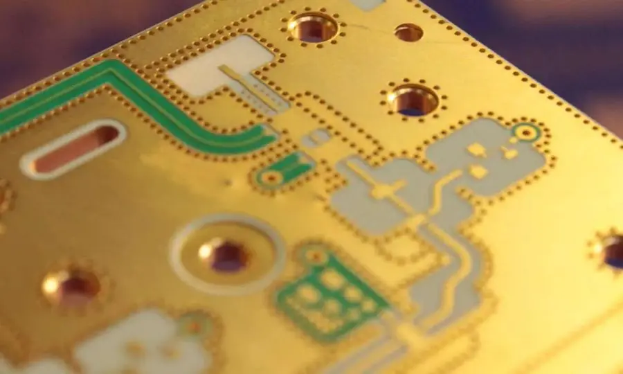


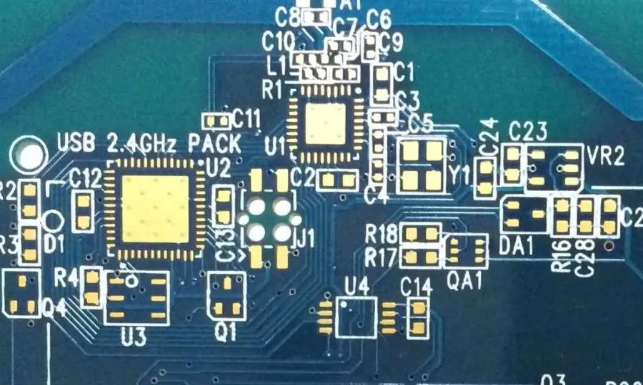

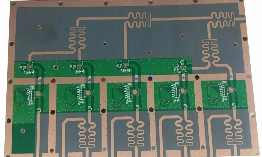


RF PCB Design Suite
Comprehensive engineering tools for high-frequency PCB design. Calculate impedance, compare materials, estimate costs, and optimize your RF designs.
85+
RF Materials
6
Calculators
77 GHz
Max Frequency
Impedance Calculator
Microstrip, Stripline, CPWG
Calculate transmission line impedance for various geometries with RF substrate materials.
Materials Database
85+ RF Substrates
Compare Rogers, Taconic, Arlon, Isola, and more with detailed electrical properties.
Cost Estimator
Instant Quotes
Get estimated manufacturing costs based on material, layers, and specifications.
Megtron 6
Dk 3.4
Df 0.002 @ 10GHz
Taconic RF-35
Dk 3.5
Df 0.0018 @ 10GHz
Isola Astra MT77
Dk 3.0
Df 0.0017 @ 10GHz
💡 Quick Tip
For frequencies above 10 GHz, consider materials with Df < 0.003 to minimize signal loss. Rogers RO3003 and Taconic TLY-5 are excellent choices for mmWave applications.
RF Materials Database
Comprehensive substrate specifications
| Material | Manufacturer | Dk @10GHz | Df @10GHz | Thickness (mm) | CTE Z (ppm/°C) | Tg (°C) | Thermal K | Max Freq | Cost Index |
|---|
Material Comparison
Select up to 4 materials
Selection Guide
Quick reference by application
🛰️ Satellite/Aerospace
Rogers RT/duroid 5880, Taconic TLY-5, Arlon CLTE-XT
📱 5G/mmWave
Rogers RO3003, Taconic TLX-8, Isola Astra MT77
🚗 Automotive Radar
Rogers RO3003, RO4835, Taconic RF-35
📶 Wi-Fi/Bluetooth
Rogers RO4350B, Megtron 6, Isola I-Tera MT40
Microstrip Impedance Calculator
Surface trace on dielectric substrate
mm
mm
mm
Target Impedance Synthesis
Calculate required trace width
Ω
mm
📐 Design Guidelines
• For 50Ω microstrip: W ≈ 2×H for εr ≈ 4
• Keep W/H between 0.5 and 4 for accurate models
• Consider via spacing for ground return path
• Edge coupling increases with narrower spacing
Stack-Up Builder
Configure your PCB layers
Stack-Up Preview
4-Layer RF/Digital Hybrid
| Layer | Type | Material | Thickness |
|---|---|---|---|
| L1 | Signal (RF) | RO4350B | 35 μm Cu |
| - | Prepreg | RO4450F | 0.1 mm |
| L2 | Ground | - | 35 μm Cu |
| - | Core | FR-4 | 1.0 mm |
| L3 | Power | - | 35 μm Cu |
| - | Prepreg | FR-4 PP | 0.2 mm |
| L4 | Signal | - | 35 μm Cu |
💡 RF Stack-Up Tips
• Place RF traces on outer layers adjacent to ground
• Use continuous ground plane under RF routing
• Consider thermal relief for RF components
• Match Dk between prepreg and core for hybrid stacks
Common RF Stack-Ups
Industry-standard configurations
2-Layer Simple RF
RO4350B
Signal-Ground, 10-20 mil core. Best for simple RF circuits, filters, antennas.
4-Layer Hybrid
RO4350B + FR-4
RF/GND/PWR/Signal. Cost-effective mixed RF/digital design.
6-Layer High-Speed
Megtron 6
S/G/S/S/G/S. High-speed digital + RF with excellent signal integrity.
mmWave 4-Layer
RO3003 + RO4450F
Ultra-low loss for 24-77 GHz automotive radar applications.
SiP/Module Substrate
Isola Astra MT77
Fine-line capable, low-loss for System-in-Package applications.
RF PCB Cost Estimator
Get instant manufacturing estimates
×
mm
Cost Breakdown
Estimated manufacturing cost
Base PCB (FR-4 equiv.)
$--
Material Premium
Layer Count
$--
Surface Finish
$--
Impedance Control
$--
Other Options
$--
Estimated Total
$--
Per Board
$--
Per sq. inch
$--
⚠️ Disclaimer
This is an estimate only. Actual costs vary by manufacturer, lead time, and specific requirements. Contact RayPCB for accurate quotes.
Material Cost Index
Relative pricing comparison
Budget
1× - 1.5×
FR-4, High-Tg FR-4
Mid-Range
2× - 3.5×
Megtron 4/6, Nelco N4000
Premium RF
4× - 6×
RO4350B, RO4003C, RO3003
Ultra Low-Loss
6× - 10×
RT/duroid 5880, TLY-5
RF Design Formulas
Essential equations
Wavelength
λ₀ = c / f = 299.792 / f(GHz) mm
λg = λ₀ / √εeff
Skin Depth
δ = √(ρ / πfμ)
For copper: δ ≈ 66/√f(MHz) μm
Dielectric Loss
αd = 27.3 × (εr/εeff) × (εeff-1)/(εr-1) × (tan δ/λ₀) dB/length
Propagation Delay
tpd = √εeff / c ≈ 3.33√εeff ps/mm
Via Inductance (Approx)
L ≈ 5.08h[ln(4h/d) + 1] nH
h = via height (in), d = via diameter (in)
Design Guidelines
Best practices for RF PCB
📐 Trace Width Rules
• 50Ω microstrip: W ≈ 1.8-2× substrate height (εr≈4)
• Keep W/H ratio between 0.5 and 4
• Match trace widths at transitions
🔗 Via Design
• Ground via spacing < λ/10
• Via stub length < λ/20 for mmWave
• Use back-drilling for high-frequency
• Multiple vias reduce inductance
🌐 Grounding
• Solid ground plane under RF traces
• Avoid splits/slots under RF routing
• Via stitch ground around RF sections
• Star ground for mixed-signal
📏 Layout Tips
• Keep RF traces short and direct
• 45° or curved bends, no 90° corners
• Maintain consistent trace width
• Isolate RF from digital/power
Unit Conversion Reference
Common conversions for RF design
Length
| 1 mil | = | 0.0254 mm |
| 1 mm | = | 39.37 mil |
| 1 inch | = | 25.4 mm |
| 1 μm | = | 0.0394 mil |
Copper Weight
| 0.5 oz | = | 17.5 μm |
| 1 oz | = | 35 μm |
| 2 oz | = | 70 μm |
| 3 oz | = | 105 μm |
Frequency
| 1 GHz | = | 1000 MHz |
| λ @ 1 GHz | = | 300 mm |
| λ @ 10 GHz | = | 30 mm |
| λ @ 77 GHz | = | 3.9 mm |
Manufacturer Resources
Official material datasheets