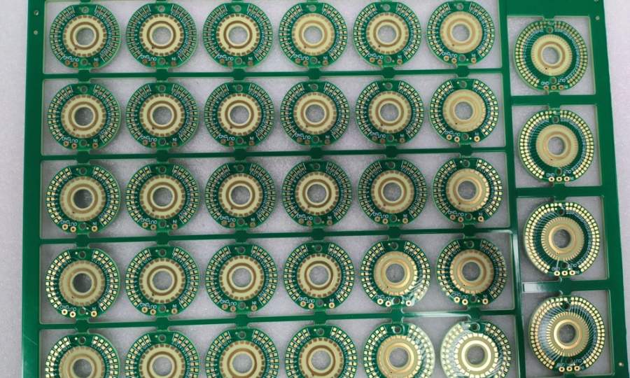
Hard gold plating is an electroplated surface finish that deposits a durable gold alloy coating onto specific PCB areas, providing exceptional wear resistance and electrical conductivity.
After working with circuit boards for over a decade, I can tell you that choosing the right surface finish can make or break your product. Gold plating PCB has become my go-to recommendation for clients who need reliability, excellent conductivity, and long-term performance. Whether you’re designing aerospace electronics, medical devices, or high-frequency communication systems, understanding gold plating options will help you make better decisions for your next project.
In this comprehensive guide, I’ll walk you through everything you need to know about gold plating on printed circuit boards, from the fundamental processes to real-world application considerations.
Gold plating PCB is an electrochemical process that deposits a thin layer of gold onto the copper traces and contact points of circuit boards. The gold layer serves as a protective barrier that prevents oxidation and corrosion while providing excellent electrical conductivity.
The process typically involves several key steps. First, the copper surface gets cleaned and prepared thoroughly. Then, a nickel layer is electroplated onto the copper surface to create a strong adhesion base. Finally, a thin layer of gold is electroplated over the nickel layer. The resulting gold-plated surface is extremely thin, typically ranging from 0.03 to 2.5 microns depending on the application requirements.
From my experience working on hundreds of PCB projects, gold plating offers three primary advantages that other surface finishes simply cannot match: superior corrosion resistance, excellent electrical conductivity, and exceptional longevity.


Before diving into the technical details, let me explain why gold plating PCB matters in the first place.
Bare copper PCBs have excellent electrical conductivity but poor corrosion resistance. Exposed copper readily oxidizes when contacted by oxygen and moisture, developing a dark tarnish within days of exposure to air. This oxidation creates a resistive oxide layer that degrades electrical performance and makes soldering difficult.
Gold plating completely eliminates copper oxidation, maintaining electrical properties indefinitely. I’ve tested boards that sat in storage for years and still performed perfectly because of their gold finish.
Gold offers stable, low-contact resistance and high conductivity, making it ideal for usage on a PCB’s connecting points. The superior conductivity ensures signal integrity, especially important for high-frequency applications where even minor resistance variations can cause problems.
For applications requiring long-term storage or operation in corrosive environments, gold plating provides unmatched protection. Gold-plated PCBs can withstand thousands of insertion cycles without significant wear, making them perfect for connectors and edge fingers.
RayPCB Engineering Tools
Based on your insertion cycle requirements, the recommended gold thickness ensures optimal wear resistance and electrical performance for your application.
• Minimize gold finger area where possible
• Consider ENIG for areas not requiring insertion wear resistance
• Order in larger quantities for volume discounts
• Standard thicknesses (30-50 μ") are more cost-effective
| Parameter | Specification |
|---|---|
| Gold Thickness | 1.27 μm (50 μ") |
| Nickel Underplate | 3.8 - 5.0 μm (150-200 μ") |
| Gold Purity | 99.7% min (Hard Gold with Co/Ni) |
| Hardness | 130-200 HV (Knoop) |
| Insertion Cycles | 500-1000 cycles |
| Contact Resistance | < 20 mΩ initial |
Design Note: Hard gold areas should be kept separate from ENIG/ENEPIG surface finish areas. Use solder mask to define boundaries clearly. Ensure adequate clearance from solder joints.
| Property | Hard Gold (Electroplated) | Soft Gold (ENIG/ENEPIG) |
|---|---|---|
| Hardness | 130-200 HV | 60-85 HV |
| Purity | 99.7% (Co or Ni alloyed) | 99.9%+ pure |
| Typical Thickness | 0.5 - 2.5 μm | 0.05 - 0.15 μm |
| Wear Resistance | Excellent | Poor |
| Solderability | Fair (not recommended) | Excellent |
| Wire Bonding | Not suitable | Excellent |
| Cost | Higher (area-dependent) | Lower (full surface) |
| Primary Use | Edge connectors, contacts | SMD pads, BGA |
| Standard | Description | Key Requirements |
|---|---|---|
| IPC-4552 | ENIG Specification | Au: 0.05-0.23 μm, Ni: 3-6 μm |
| IPC-4556 | ENEPIG Specification | Au: 0.03-0.08 μm, Pd: 0.05-0.15 μm |
| MIL-G-45204 | Gold Plating (Military) | Type I/II/III, Class 0-4 |
| ASTM B488 | Electrodeposited Gold | Type I-III, Grades A-D |
• XRF Analysis: Non-destructive thickness measurement
• Tape Test: Adhesion verification per ASTM D3359
• Microhardness: Knoop or Vickers hardness testing
• Porosity Test: Nitric acid vapor or electrographic
• Contact Resistance: Four-point probe measurement
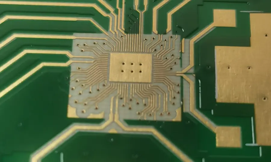
Understanding the different types of gold plating PCB options is crucial for selecting the right finish for your specific application. Each method has distinct characteristics that make it suitable for different use cases.
ENIG, or Electroless Nickel Immersion Gold, is currently the most widely used gold surface finish in the PCB industry. The process involves depositing a nickel layer through an autocatalytic chemical reaction, followed by a thin gold layer through immersion.
ENIG Layer Composition:
The nickel layer serves as a barrier to prevent copper diffusion, while the thin gold layer protects the nickel during storage and provides excellent solderability. ENIG creates a smooth, flat surface that’s perfect for fine-pitch components, BGAs, and other high-density assemblies.
Key Characteristics of ENIG:
However, ENIG does have limitations. The gold layer is relatively thin and soft, making it unsuitable for areas requiring frequent mechanical contact. There’s also a potential issue called “black pad” where nickel corrosion can occur if process control isn’t properly maintained.
Hard gold plating, also known as electrolytic hard gold, involves depositing a thicker layer of gold through an electroplating process. Unlike ENIG, hard gold is alloyed with small amounts of cobalt or nickel (typically 5-10%) to enhance hardness and wear resistance.
Hard Gold Layer Composition:
The thicker gold layer and alloying metals make hard gold extremely durable. It can withstand up to 1,000 insertion cycles without significant wear, making it ideal for edge connectors (gold fingers), keypads, and other high-wear areas.
Key Characteristics of Hard Gold:
The main drawback of hard gold plating is cost. The thicker gold layer and more complex electroplating process make it significantly more expensive than ENIG. Additionally, the alloying elements that provide hardness also reduce solderability.
ENEPIG adds a palladium layer between the nickel and gold layers, creating a three-layer metallic coating. This surface finish addresses some of ENIG’s limitations while providing additional benefits.
ENEPIG Layer Composition:
The palladium layer prevents nickel from oxidizing before gold immersion (which causes black pad defects), improves solder reliability, and provides better wire bonding capability.
Key Characteristics of ENEPIG:
ENEPIG is often called a “universal” finish because it can handle almost any assembly process. However, the additional palladium layer increases cost, and not all PCB manufacturers have the capability to process ENEPIG.
Soft gold plating uses pure gold (99.9%) without alloying metals. This creates a softer, more malleable finish that’s excellent for wire bonding but poor for wear resistance.
Soft Gold Characteristics:
Selective gold plating applies hard gold only to specific areas of the PCB that require wear resistance, while other areas use different finishes like ENIG or OSP. This approach optimizes cost while providing the right finish where it’s needed most.
Common applications include gold fingers on edge connectors combined with ENIG on soldering pads. This requires precise masking during manufacturing and adds complexity to the production process.
| Feature | ENIG | Hard Gold | ENEPIG | Soft Gold |
|---|---|---|---|---|
| Gold Thickness | 0.05-0.125 µm | 0.76-2.5 µm | 0.05-0.15 µm | 0.03-0.1 µm |
| Nickel Thickness | 3-6 µm | 2.5-5 µm | 3-5 µm | 3-6 µm |
| Hardness (HK) | 20-100 | 130-200 | 50-90 | 20-60 |
| Wear Resistance | Low | Excellent | Moderate | Very Low |
| Solderability | Excellent | Poor | Excellent | Good |
| Wire Bonding | Good | Poor | Excellent | Excellent |
| Insertion Cycles | <50 | 1000+ | 100-200 | <20 |
| Relative Cost | Medium | High | High | Medium |
| Black Pad Risk | Possible | None | None | Possible |
| RoHS Compliant | Yes | Yes | Yes | Yes |

Understanding the gold plating PCB process helps you specify requirements correctly and troubleshoot potential issues. Here’s how the typical electroplating process works for hard gold plating on gold fingers:
Before any plating can occur, the PCB undergoes thorough cleaning. Any contaminants like oils, dust, or oxides on the copper pads interfere with adhesion during plating. The board is cleaned using alkaline solutions or micro-etching to remove impurities and create a uniform surface.
After chemical cleaning, mechanical abrasion further cleans the PCB pads. The board is then rinsed with water and a final deionized water rinse removes any remaining chemicals. Even minor residues can lead to uneven plating or poor bonding between layers.
For selective gold plating, areas that shouldn’t receive gold are masked with protective tape or photoresist. This is especially important for gold fingers where only the connector edges need the hard gold finish.
A layer of nickel is electroplated onto the copper pads. Nickel plating serves as a barrier layer, preventing copper from migrating into the gold coating, which could cause corrosion or reduced conductivity over time.
Typical nickel thickness ranges from 2.5 to 5 microns (100-200 microinches). The PCB is immersed in a solution containing nickel salts, and an electric current deposits a uniform nickel layer on the prepared surfaces.
With the nickel layer in place, gold is electroplated onto the surface. The board is immersed in a gold plating bath containing gold salts (typically potassium gold cyanide), and electrical current deposits gold onto the nickel layer.
For hard gold, the bath also contains alloying metals like cobalt. Plating thickness is controlled by adjusting current density, bath composition, and plating time. Typical hard gold thickness ranges from 30 to 50 microinches for general applications, up to 100 microinches for high-wear requirements.
After plating, the boards undergo thorough inspection. Key tests include:
The masking materials are removed, and the board continues through normal manufacturing steps like solder mask application and final assembly.
Proper design is crucial for manufacturing reliable gold finger PCBs. Here are the essential design rules I always follow:
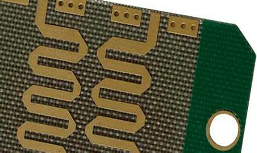
Connector edges are beveled at specific angles (typically 20-45 degrees) to facilitate smooth insertion into mating connectors. Beveling prevents damage during insertion and reduces wear on both the connector and the mated slot.

Compliance with industry standards ensures quality and reliability. Here are the key standards governing gold plating PCB:
This standard covers requirements for electroless nickel immersion gold plating. Key specifications include:
IPC-4552B introduced quantifiable methods for measuring nickel corrosion frequency and severity, helping manufacturers control quality more effectively.
This standard defines requirements for the three-layer ENEPIG finish:
This standard includes specifications for hard gold plating:
For military and aerospace applications, this standard specifies:
Cost is always a factor in surface finish selection. Here’s what affects gold plating PCB pricing:
| Factor | Impact on Cost |
|---|---|
| Gold thickness | Higher thickness = higher cost (gold is expensive) |
| Plating area | Larger gold areas increase material cost |
| Selective vs. full plating | Selective plating adds processing steps |
| Volume | Higher volumes reduce per-unit cost |
| Complexity | Multi-layer boards cost more to plate |
| IPC Class | Higher reliability classes require tighter tolerances |
As a rough guide, here’s how different finishes compare cost-wise:
The actual premium depends heavily on gold prices, which fluctuate with the commodities market.
Gold plating PCB finds use across numerous industries where reliability and performance are critical.
Gold-plated PCBs are standard in aerospace and military applications where reliability is non-negotiable. Aircraft avionics, satellite communications, and military guidance systems use gold plating to ensure long-term functionality in demanding environments. The extended shelf life is particularly valuable in defense applications where equipment may be stored for years before deployment.
Implantable and external medical devices require exceptional biocompatibility and long-term reliability. Gold plating provides corrosion resistance that prevents metal ion leaching that could trigger allergic reactions or tissue damage. Pacemakers, hearing aids, surgical instruments, and diagnostic equipment commonly employ gold plating.
While cost constraints limit gold plating use in low-end products, premium consumer electronics benefit from gold plating in high-wear areas. Memory sticks, graphics cards, and other expansion cards use gold fingers for reliable connections to motherboards.
High-frequency communication equipment requires stable, low-resistance connections. Gold plating PCB ensures signal integrity in 5G infrastructure, satellite systems, and networking equipment.
Industrial control systems, automation equipment, and test instruments often use gold plating for connectors and switches that see frequent use. The superior wear resistance ensures years of reliable operation.
Selecting the right gold thickness depends on your specific application. Here’s a practical guide:
| Application | Recommended Gold Thickness | Notes |
|---|---|---|
| SMD Pads (ENIG) | 0.05-0.125 µm | Standard for soldering |
| Wire Bonding | 0.3+ µm (ENIG) or ENEPIG | Thicker gold needed |
| Low-frequency connectors | 10-20 microinches | Minimal wear |
| General gold fingers | 30 microinches | IPC Class 2/3 minimum |
| High-wear connectors | 50 microinches | Thousands of cycles |
| Extreme applications | 50-100 microinches | Military, aerospace |
Making the right choice between different gold plating PCB options can be challenging. Here’s my decision framework based on years of practical experience:
Select ENIG when your primary concern is solderability and you have fine-pitch components like BGAs, QFPs, or CSPs. ENIG works well for products that won’t experience mechanical wear on the plated surfaces. It’s cost-effective for mass production and provides excellent shelf life.
Ideal applications include consumer electronics, telecommunications equipment, and any product with complex SMD assembly requirements. The flat, coplanar surface makes ENIG perfect for high-density interconnect (HDI) boards.
Choose hard gold plating when durability matters more than solderability. Edge connectors, switch contacts, test points that see repeated probe contact, and keyboard contacts all benefit from hard gold’s wear resistance.
I always recommend hard gold for any connector expected to see more than 100 insertion cycles. The upfront cost premium pays off quickly when you consider the cost of field failures from worn-out contacts.
ENEPIG makes sense when you need wire bonding capability or when black pad risk is unacceptable. Medical devices, aerospace electronics, and high-reliability applications often specify ENEPIG for its superior performance characteristics.
If your product requires both excellent solderability and wire bonding, ENEPIG is really the only practical choice. The palladium layer provides insurance against nickel corrosion issues that can plague ENIG in some environments.
Selective gold plating combines the best of multiple finishes. Use hard gold on edge connectors while applying ENIG to SMD pads. This approach optimizes cost without compromising performance where it matters.
The added manufacturing complexity requires clear communication with your PCB fabricator. Provide detailed drawings showing exactly which areas require each finish type.

Even with proper processes, problems can occur. Here are issues I’ve encountered and how to address them:
Black pad occurs when nickel corrodes before or after gold immersion, creating weak solder joints. Prevention involves proper process control including bath chemistry monitoring, temperature control, and limiting time between plating steps. Using ENEPIG instead of ENIG eliminates this risk.
Inadequate surface preparation causes poor adhesion between layers. Ensure thorough cleaning and proper activation before plating. Adhesion testing per ASTM B571 should be part of quality control.
Inconsistent gold thickness results from non-uniform current distribution during electroplating. Proper anode placement, bath agitation, and current density control minimize variations. XRF measurement at multiple points verifies uniformity.
Surface defects can result from contamination, improper bath chemistry, or incorrect plating parameters. Regular bath analysis and maintenance prevents most issues.
Here are valuable resources for further learning:
To achieve optimal results with hard gold plating in PCB design, follow these best practices tailored for engineers and designers.
Specify Plating Areas Clearly: Use design files to indicate exactly where hard gold plating is needed, such as on edge connectors or specific pads.
Documentation Requirements:
Choose the Right Thickness: Match the gold thickness to the application’s wear and environmental requirements. For instance, use 0.8-1.3 microns for moderate wear and up to 2.5 microns for high-cycle applications.
Ensure Proper Nickel Underlayer: A uniform nickel layer of 3-6 microns is critical for adhesion and durability. Specify this in your design requirements to avoid issues like gold peeling.
Collaborate with Manufacturers Early: Work closely with your PCB fabrication partner during the design phase to confirm that your hard gold plating requirements are feasible and cost-effective.
Partnership Benefits:
Implement comprehensive quality control throughout the design and manufacturing process:
QA Checkpoints:
ENIG uses a chemical process to deposit a thin gold layer (0.05-0.125 µm) over electroless nickel, making it excellent for soldering but poor for wear resistance. Hard gold plating uses an electroplating process to deposit a thicker gold layer (0.76-2.5 µm) alloyed with cobalt, making it extremely durable for connectors but unsuitable for soldering. Choose ENIG for SMD assembly and hard gold for edge connectors and high-wear contacts.
For most applications, 30 microinches (0.76 µm) of hard gold over 100-150 microinches of nickel meets IPC Class 2 and Class 3 requirements. High-reliability applications like military or aerospace may require 50 microinches (1.27 µm) or more. Consumer electronics with fewer insertion cycles can use thinner plating (10-20 microinches) to reduce costs.
Hard gold plating is not recommended for soldering. The cobalt or nickel alloying elements that provide wear resistance interfere with solder wetting and can cause brittle solder joints. For surfaces requiring both wear resistance and solderability, use selective plating with hard gold on contacts and ENIG or ENEPIG on SMD pads.
Black pad occurs when nickel corrodes during the immersion gold process or afterward due to phosphorus segregation at the nickel surface. The defect appears as a dark layer between nickel and gold that causes solder joint failures. Prevention requires proper process control including bath chemistry, temperature, and dwell time. Switching to ENEPIG eliminates black pad risk because the palladium layer protects nickel during gold immersion.
Yes, all gold plating PCB processes including ENIG, ENEPIG, and hard gold are RoHS compliant. Gold, nickel, and palladium are not restricted substances under RoHS regulations. Gold plating has actually become more popular since RoHS implementation because it provides a reliable lead-free surface finish suitable for lead-free soldering processes.
Selecting the right gold plating PCB finish requires balancing performance requirements, application demands, and budget constraints. ENIG remains the most popular choice for general SMD assembly due to its excellent solderability and reasonable cost. Hard gold plating is essential for edge connectors and high-wear applications. ENEPIG offers the best of both worlds for demanding applications willing to pay the premium.
Whatever finish you choose, proper design, specification to IPC standards, and working with experienced manufacturers ensures your gold-plated PCBs will deliver the reliability and performance your products demand.
If you have questions about gold plating for your specific application, work closely with your PCB manufacturer early in the design process. Getting the surface finish right from the start saves time, money, and headaches down the road.