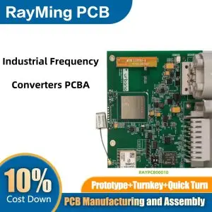
In the rapidly evolving world of electronics, the demand for high-performance circuits operating at increasingly higher frequencies continues to grow. This trend has led to the development and widespread use of High Frequency (HF) Printed Circuit Boards (PCBs). These specialized PCBs play a crucial role in various applications, from telecommunications to aerospace technology. In this comprehensive guide, we’ll explore the intricacies of High Frequency PCBs, their properties, materials, design considerations, and applications.
What is High Frequency (HF) PCB?
High Frequency PCBs are specialized printed circuit boards designed to handle signals operating at frequencies typically ranging from 500 MHz to 2 GHz and beyond. These PCBs are engineered to maintain signal integrity and minimize losses at these high frequencies, making them essential for RF (Radio Frequency) and microwave applications.
Unlike standard PCBs, HF PCBs are built using specialized materials and design techniques to address the unique challenges posed by high-frequency signals, such as:
- Signal loss
- Electromagnetic interference (EMI)
- Crosstalk
- Impedance mismatches
High Frequency PCBs are critical components in various industries, including telecommunications, aerospace, defense, and medical equipment manufacturing.
Z₀ = (87 / √(εr + 1.41)) × ln(5.98H / (0.8W + T)) Ω
Effective Dielectric Constant:
εeff = (εr + 1)/2 + (εr – 1)/2 × (1 + 12H/W)^(-0.5)
| Material | Dk @ 10GHz | Df @ 10GHz | Tg (°C) | CTE Z | Freq Range | Cost Index |
|---|---|---|---|---|---|---|
| Standard FR-4 | 4.2 – 4.5 | 0.020 – 0.025 | 130-140 | 50-70 ppm | < 3 GHz | |
| High-Tg FR-4 | 4.0 – 4.3 | 0.018 – 0.022 | 170-180 | 45-60 ppm | < 5 GHz | |
| Megtron 6 | 3.7 – 4.0 | 0.004 – 0.006 | 185 | 30-40 ppm | 3-15 GHz | |
| RO4003C | 3.38 ±0.05 | 0.0027 | 280+ | 46 ppm | 10-40 GHz | |
| RO4350B | 3.48 ±0.05 | 0.0037 | 280+ | 32 ppm | 10-40 GHz | |
| RO3003 | 3.00 ±0.04 | 0.0013 | N/A | 24 ppm | > 40 GHz | |
| Taconic TLY | 2.2 ±0.02 | 0.0009 | N/A | 280 ppm | > 77 GHz | |
| Isola I-Tera MT40 | 3.45 | 0.0031 | 200 | 35 ppm | 10-25 GHz |
Cross-Section View
• Maintain consistent trace impedance (typically 50Ω single-ended, 100Ω differential)
• Keep trace width constant throughout signal path
• Avoid 90° corners – use 45° miters or curved traces
• Use ground coplanar waveguide (GCPW) for better isolation above 20 GHz
• Route critical RF traces on outer layers when possible
• Use back-drilling to eliminate via stubs above 10 GHz
• Place ground vias within 0.5mm of signal vias
• Minimize via inductance with larger pad sizes
• Use blind/buried vias to reduce stub length
• Consider via-in-pad for BGA breakout (filled and capped)
• Use solid ground planes – avoid splitting under RF traces
• Place decoupling capacitors close to IC power pins
• Use multi-value capacitor networks for broadband decoupling
• Keep power plane cutouts away from RF signal paths
• Consider stitching capacitors for ground plane connections
• Use via fencing around sensitive RF traces
• Implement guard traces for high-isolation requirements
• Maintain minimum 3× trace width spacing between signals
• Consider embedded shielding for critical circuits
• Use edge-plated shielding for maximum isolation
• Minimize trace length between RF components
• Group RF circuits by function (LNA, mixer, filter)
• Separate analog, digital, and RF sections
• Orient components to minimize trace bends
• Consider thermal management for power amplifiers
• Specify tight Dk tolerance (±2% for RF layers)
• Request impedance testing with TDR
• Define copper roughness requirements (VLP/HVLP)
• Use symmetrical stackup to prevent warpage
• Consider material availability for production volumes
| Band | Frequency Range | Typical Applications | Recommended Materials | Max Df |
|---|---|---|---|---|
| L-Band | 1-2 GHz | GPS, Cellular | High-Tg FR-4, Megtron | 0.015 |
| S-Band | 2-4 GHz | WiFi, Radar | Megtron 6, I-Tera | 0.008 |
| C-Band | 4-8 GHz | 5G Sub-6, Satellite | RO4350B, Megtron 7 | 0.005 |
| X-Band | 8-12 GHz | Radar, Point-to-Point | RO4003C, RO4835 | 0.004 |
| Ku-Band | 12-18 GHz | Satellite Comm | RO3003, RT/duroid | 0.003 |
| K/Ka-Band | 18-40 GHz | 5G mmWave, Radar | RO3003, Taconic TLY | 0.002 |
| V-Band | 40-75 GHz | 60 GHz WiGig | LCP, PTFE | 0.0015 |
| W-Band | 75-110 GHz | Automotive Radar | LCP, Pure PTFE | 0.001 |
Learn more about:
Properties of High Frequency PCBs

The performance of High Frequency PCBs is largely determined by their material properties. Let’s explore the key characteristics that make these PCBs suitable for high-frequency applications:
1. Low Dielectric Constant (Dk)
The dielectric constant, also known as relative permittivity, is a measure of a material’s ability to store electrical energy in an electric field. For HF PCBs, a low Dk is desirable because it:
- Reduces signal propagation delay
- Minimizes crosstalk between adjacent traces
- Improves overall signal integrity
Typical Dk values for HF PCB materials range from 2.2 to 3.5, compared to 4.0-4.5 for standard FR-4 materials.
2. Low Dissipation Factor (Df)
The dissipation factor, also called loss tangent, represents the amount of energy lost as signals propagate through the material. A low Df is crucial for HF PCBs because it:
- Reduces signal attenuation
- Minimizes power loss
- Improves the overall efficiency of the circuit
HF PCB materials typically have Df values in the range of 0.001 to 0.003, significantly lower than the 0.02 typical of FR-4 materials.
3. Low Dimensional Stability
Dimensional stability refers to a material’s ability to maintain its physical dimensions under varying environmental conditions. HF PCBs require excellent dimensional stability to:
- Ensure consistent electrical performance across temperature ranges
- Maintain precise impedance control
- Prevent warpage and delamination
Materials used in HF PCBs often have a coefficient of thermal expansion (CTE) closely matched to that of copper, minimizing stress on the board during temperature fluctuations.
4. Low Moisture Absorption
Moisture absorption can significantly affect the electrical properties of PCB materials. HF PCBs use materials with low moisture absorption rates to:
- Maintain stable dielectric properties
- Prevent changes in impedance due to moisture uptake
- Enhance long-term reliability, especially in humid environments
5. Chemical Resistance
HF PCBs often operate in challenging environments, necessitating good chemical resistance. This property ensures:
- Durability during manufacturing processes
- Resistance to degradation from environmental factors
- Long-term reliability in various operating conditions
Materials Used for High Frequency PCB
The choice of material is critical in HF PCB design. Here are some of the most commonly used materials for High Frequency PCBs:
1. Rogers 4350B
- Dk: 3.48 ± 0.05 (10 GHz)
- Df: 0.0037 (10 GHz)
- Applications: Cellular base station antennas, power amplifiers
2. Rogers 4003C
- Dk: 3.38 ± 0.05 (10 GHz)
- Df: 0.0027 (10 GHz)
- Applications: Satellite communications, phased array antennas
3. Panasonic Megtron6
- Dk: 3.4 (1 GHz)
- Df: 0.002 (1 GHz)
- Applications: High-speed digital, RF, and microwave applications
4. Rogers RO3003
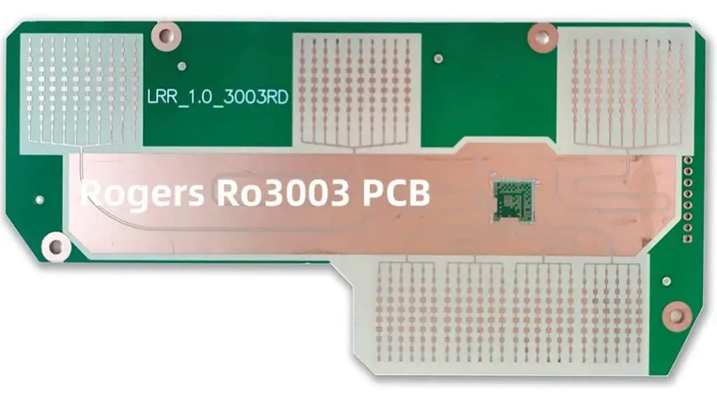

- Dk: 3.00 ± 0.04 (10 GHz)
- Df: 0.0010 (10 GHz)
- Applications: Millimeter-wave circuits, automotive radar
5. Rogers RO3006
- Dk: 6.15 ± 0.15 (10 GHz)
- Df: 0.0025 (10 GHz)
- Applications: GPS patch antennas, satellite communications
6. Rogers RO3010
- Dk: 10.2 ± 0.30 (10 GHz)
- Df: 0.0022 (10 GHz)
- Applications: Patch antennas, RF/microwave circuits requiring high Dk
7. Taconic RF-35
- Dk: 3.50 ± 0.05 (10 GHz)
- Df: 0.0018 (10 GHz)
- Applications: Power amplifiers, LNAs, filters
8. Taconic TLX
- Dk: 2.55 ± 0.04 (10 GHz)
- Df: 0.0019 (10 GHz)
- Applications: Low-loss microstrip and stripline circuits
9. Rogers 5880
- Dk: 2.20 ± 0.02 (10 GHz)
- Df: 0.0009 (10 GHz)
- Applications: Aerospace and defense, millimeter-wave applications
10. Taconic TLC
- Dk: 3.00 ± 0.03 (10 GHz)
- Df: 0.0030 (10 GHz)
- Applications: Cost-effective alternative for less demanding RF applications
Design Tips of High-Frequency PCB

Designing High Frequency PCBs requires careful consideration of various factors to ensure optimal performance. Here are some essential design tips:
1. Routing Method
- Use smooth curves instead of sharp 90-degree turns to minimize reflections
- Implement differential pair routing for high-speed signals
- Maintain consistent trace widths to control impedance
2. Routing Length
- Keep high-frequency signal traces as short as possible
- Match trace lengths for differential pairs and clock signals
- Use serpentine routing for length matching when necessary
3. Use Less Number of Vias
- Minimize the use of vias in high-frequency signal paths
- When vias are necessary, use back-drilling to reduce stub length
- Consider using buried or blind vias for critical high-frequency connections
4. Avoiding Crosstalk
- Maintain adequate spacing between high-frequency traces
- Use ground planes and guard traces to isolate sensitive signals
- Avoid parallel routing of high-frequency signals over long distances
5. Implement Shorter Leads Between the Pins in a High-Frequency Circuit
- Minimize lead lengths to reduce parasitic inductance and capacitance
- Use surface mount components whenever possible
- Consider using embedded components for critical high-frequency circuits
6. Add High-Frequency Decoupling Capacitors to the Power Supply Pins of IC Chips
- Place decoupling capacitors as close as possible to IC power pins
- Use a combination of capacitor values to cover a wide frequency range
- Implement power plane sandwiches to reduce power distribution inductance
7. Isolate the Ground of High-Frequency Digital Signals and the Ground of Analog Signals
- Use separate ground planes for digital and analog sections
- Implement a single-point ground connection between digital and analog grounds
- Consider using split planes for mixed-signal designs
8. Avoid the Formation of Loops Resulting from Routing
- Minimize current loop areas in high-frequency circuits
- Use solid ground planes to provide low-impedance return paths
- Avoid creating slots or gaps in ground planes under high-frequency traces
9. Type of Transmission Line
- Choose appropriate transmission line structures (microstrip, stripline, coplanar waveguide) based on the application
- Maintain consistent impedance throughout the signal path
- Use electromagnetic field solvers to optimize transmission line structures
10. Adopt Fly-by Topology/Daisy Chain Routing for DDR4
- Implement fly-by topology for memory interfaces to reduce reflections
- Use termination resistors at the end of each fly-by chain
- Carefully match trace lengths within each byte lane
11. Adopt the 20H Rule to Minimize Plane Coupling
- Maintain a minimum separation of 20 times the dielectric thickness between adjacent plane layers
- Use cross-hatched planes to reduce plane resonances
- Consider using multiple thin dielectric layers instead of a single thick layer
12. Ensure Proper Signal Impedance Matching
- Calculate and maintain proper trace widths for desired impedance
- Use impedance-controlled PCB fabrication processes
- Implement proper termination techniques for high-frequency signals
HF PCB Design Considerations


Designing High Frequency PCBs involves addressing several critical factors to ensure optimal performance:
1. Select Low Profile Copper-Dielectric Interface
- Use low-profile copper foils to minimize surface roughness
- Consider reverse-treated foils for improved adhesion without sacrificing performance
- Implement proper copper surface preparation techniques
2. Do Not Use FR4 for High-Frequency Applications
- Choose specialized high-frequency laminate materials
- Consider the trade-offs between performance and cost when selecting materials
- Use hybrid stackups with high-frequency materials only where necessary
3. Radiation
- Implement proper shielding techniques to minimize unwanted radiation
- Use ground planes and vias to create effective RF enclosures
- Consider the use of absorptive materials for critical applications
4. Absorption
- Select materials with low loss tangent to minimize signal absorption
- Account for frequency-dependent material properties in your designs
- Use thicker dielectric layers for reduced absorption in critical signal paths
5. Signal Degradation
- Minimize discontinuities in signal paths to reduce degradation
- Use proper via design and placement to maintain signal integrity
- Implement pre-emphasis and equalization techniques for long signal paths
6. Reflections
- Match impedances throughout the signal path to minimize reflections
- Use proper termination techniques for high-frequency transmission lines
- Avoid abrupt changes in trace width or layer transitions
7. Coupling
- Maintain proper spacing between high-frequency traces to minimize coupling
- Use guard traces and ground planes to isolate sensitive signals
- Implement differential signaling for improved noise immunity
8. EMI/EMC Compliance
- Design with EMI/EMC compliance in mind from the start
- Use proper shielding and grounding techniques
- Consider the use of spread spectrum clocking to reduce EMI
9. Parasitic Capacitance
- Minimize pad sizes and use tear-dropping to reduce parasitic capacitance
- Carefully consider component placement to minimize unwanted coupling
- Use 3D electromagnetic simulation tools to analyze and optimize designs
10. Harmonic Distortion
- Use linear components in analog sections to minimize harmonic distortion
- Implement proper filtering techniques for power supplies
- Consider the use of balanced circuit topologies to cancel even-order harmonics
11. Common Mode Noise
- Use differential signaling to minimize common mode noise
- Implement common mode chokes for critical interfaces
- Maintain symmetry in differential pair routing
12. Surface Tracking
- Use conformal coatings to prevent surface tracking in high-voltage areas
- Implement proper creepage and clearance distances
- Consider the use of slot-patterning techniques for high-voltage isolation
High Frequency PCBs vs. High Speed PCBs


While often used interchangeably, High Frequency PCBs and High Speed PCBs have some distinct characteristics:
| Aspect | High Frequency PCBs | High Speed PCBs |
|---|---|---|
| Frequency Range | Typically 500 MHz to 2 GHz and beyond | Usually up to 500 MHz |
| Signal Type | Often analog or RF | Typically digital |
| Key Concerns | Signal loss, impedance control | Signal integrity, timing |
| Materials | Specialized low-loss materials | Often FR-4 or enhanced FR-4 |
| Design Focus | Minimize loss, control impedance | Manage rise times, control reflections |
Both types of PCBs require careful design considerations, but High Frequency PCBs often demand more specialized materials and manufacturing processes.
The Advantages of High Frequency PCBs
High Frequency PCBs offer several advantages for RF and microwave applications:
- Improved Signal Integrity: Low-loss materials and proper design techniques maintain signal quality at high frequencies.
- Higher Bandwidth: HF PCBs enable the transmission of more data in less time.
- Reduced Electromagnetic Interference: Proper design and materials help minimize EMI issues.
- Smaller Form Factors: HF PCBs often allow for more compact designs due to shorter wavelengths.
- Better Power Handling: Specialized materials can offer improved thermal management for high-power RF applications.
- Precision: HF PCBs provide the necessary precision for sensitive RF and microwave circuits.
- Flexibility: Various material options allow designers to optimize performance for specific applications.
The Applications of High Frequency PCBs
High Frequency PCBs find use in a wide range of applications across multiple industries:
- Telecommunications
- 5G infrastructure
- Satellite communications
- Base station equipment
- Aerospace and Defense
- Radar systems
- Electronic warfare equipment
- Satellite navigation systems
- Medical Devices
- MRI machines
- Ultrasound equipment
- Surgical robots
- Automotive
- Advanced driver assistance systems (ADAS)
- Automotive radar
- Vehicle-to-vehicle communication systems
- Test and Measurement
- Network analyzers
- Spectrum analyzers
- High-frequency oscilloscopes
- Industrial
- Industrial IoT devices
- Wireless sensor networks
- High-frequency power supplies
- Consumer Electronics
- Smartphones
- Wi-Fi routers
- Bluetooth devices
As technology continues to advance, the importance of High Frequency PCBs in enabling high-performance electronic systems will only grow. By understanding the unique properties, design considerations, and applications of these specialized PCBs, engineers and designers can create innovative solutions to meet the challenges of our increasingly connected world.